(China (Mainland))

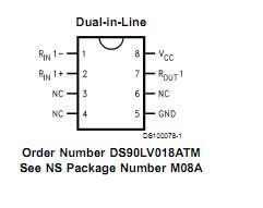
Product Summary
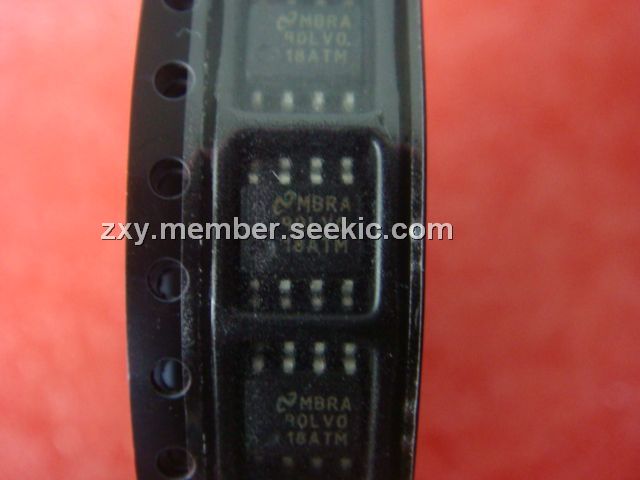
The 90LV018ATM is a single CMOS differential line receiver designed for applications requiring ultra low power dissipation, low noise and high data rates. The device is designed to support data rates in excess of 400 Mbps (200 MHz) utilizing Low Voltage Differential Signaling (LVDS) technology. The 90LV018ATM accepts low voltage (350 mV typical) differential input signals and translates them to 3V CMOS output levels. The receiver also supports open, shorted and terminated (100Ω) input fail-safe. The receiver output will be HIGH for all fail-safe conditions. The 90LV018ATM has a flow-through design for easy PCB layout. The 90LV018ATM and companion LVDS line driver provide a new alternative to high power PECL/ECL devices for high speed point-to-point interface applications.
Parametrics
90LV018ATM absolute maixmum ratings: (1)Supply Voltage (VCC): -0.3V to +4V; (2)Input Voltage (RIN+, RIN-): -0.3V to +3.9V; (3)Output Voltage (ROUT): -0.3V to (VCC + 0.3V); (4)Maximum Package Power Dissipation: +25℃; (5)M Package: 1025 mW; (6)Derate M Package: 8.2 mW/℃ above +25℃; (7)Storage Temperature Range: -65℃ to +150℃; (8)Lead Temperature Range Soldering (4 sec.): +260℃; (9)Maximum Junction Temperature: +150℃; (10)ESD Rating (HBM 1.5 k-, 100 pF): ≥ 7 kV; (11)(EIAJ 0Ω, 200 pF): ≥ 500 V.
Features
90LV018ATM features: (1)>400 Mbps (200 MHz) switching rates; (2)50 ps differential skew (typical); (3)2.5 ns maximum propagatiodelay; (4)3.3V power supply design; (5)Flow-through pinout; (6)Power dowhigh impedance oLVDS inputs; (7)Low Power desig(18mW @ 3.3V static); (8)Interoperable with existing 5V LVDS networks; (9)Accepts small swing (350 mV typical) differential signal levels; (10)Supports open, short and terminated input fail-safe; (11)Conforms to ANSI/TIA/EIA-644 Standard; (12)Industrial temperature operating range (-40℃ to +85℃); (13)Available iSOIC package.
Diagrams