(China (Mainland))

Product Summary
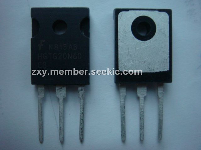
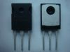
The HGTG20N60C3 MOS is a high voltage switching device combining the best features of MOSFETs and bipolar transistors. The device has the high input impedance of a MOSFET and the low on-state conduction loss of a bipolar transistor. The much lower on-state voltage drop varies only moderately between 25℃ and 150℃. The HGTG20N60C3 is ideal for many high voltage switching applications operating at moderate frequencies where low conduction losses are essential, such as: AC and DC motor controls, power supplies and drivers for solenoids, relays and contactors.
Parametrics
HGTG20N60C3 absolute maximum ratings: (1)Collector to Emitter Voltage: BVCES 600 V; (2)Collector Current Continuous, At TC = 25℃, IC25: 45 A; At TC = 110℃, IC110: 20 A; (3)Collector Current Pulsed, ICM: 300 A; (4)Gate to Emitter Voltage Continuous VGES: ±20 V; (5)Gate to Emitter Voltage Pulsed, VGEM: ±30 V; (6)Switching Safe Operating Area at TJ = 150℃, SSOA 20A at 600V; (7)Power Dissipation Total at TC = 25℃: PD 164 W; (8)Power Dissipation Derating TC > 25℃: 1.32 W/℃; (9)Reverse Voltage Avalanche Energy: EARV 100 mJ; (10)Operating and Storage Junction Temperature Range, TJ, TSTG -55 to 150 ℃; (11)Maximum Temperature for Soldering; (12)Leads at 0.063in (1.6mm) from Case for 10s, TL: 300℃; (13)Package Body for 10s, see Tech Brief 334, Tpkg: 260℃; (14)Short Circuit Withstand Time (Note 2) at VGE = 12V, tSC: 4 μs; (15)Short Circuit Withstand Time (Note 2) at VGE = 10V, tSC: 10μs.
Features
HGTG20N60C3 features: (1)45A, 600V, TC = 25℃; (2)600V Switching SOA Capability; (3)Typical Fall Time: 108ns at TJ = 150℃; (4)Short Circuit Rating; (5)Low Conduction Loss; (6)Related Literature.
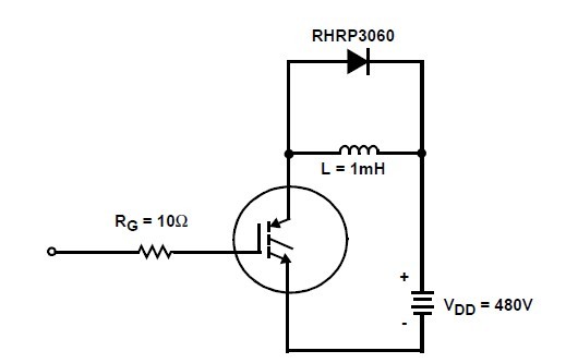
Diagrams
| Image | Part No | Mfg | Description |  |
Pricing (USD) |
Quantity | ||||
|---|---|---|---|---|---|---|---|---|---|---|
 |
 HGTG20N60C3 |
Other |
|
Data Sheet |
Negotiable |
|
||||
 |
HGTG20N60C3D |
Fairchild Semiconductor |
IGBT Transistors UFS 20A 600V N-Ch |
Data Sheet |
Negotiable |
|
||||
|
HGTG20N60C3R |
Other |
|
Data Sheet |
Negotiable |
|
||||