(China (Mainland))

Product Summary
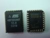
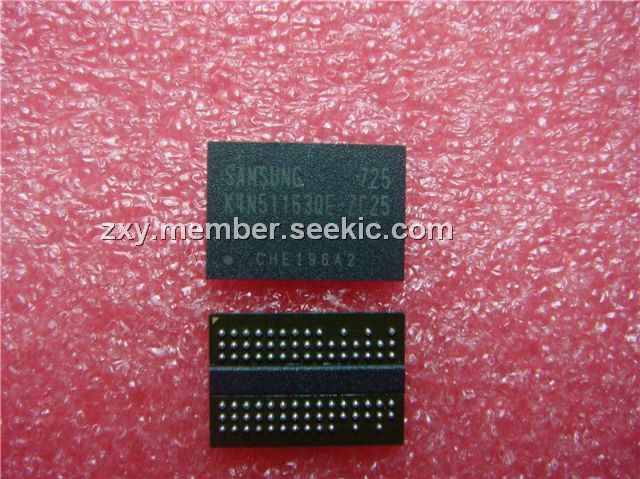
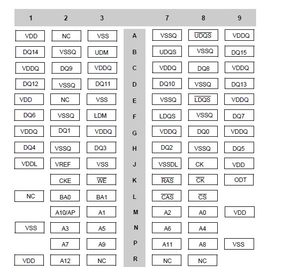
The K4N51163QE-ZC25 is a kind of 512Mb gDDR2 SDRAM chip, which is organized as 8Mbit x 16 I/O x 4banks banks device. This synchronous device achieve high speed graphic double-data-rate transfer rates of up to 500MHz for general applications. The K4N51163QE-ZC25 is designed to comply with the following key gDDR2 SDRAM features such as posted CAS with additive latency, write latency = read latency - 1, Off-Chip Driver(OCD) impedance adjustment and On Die Termination. All of the control and address inputs are synchronized with a pair of externally supplied differential clocks. Inputs are latched at the cross point of differential clocks (CK rising and CK falling). All I/Os are synchronized with a pair of bidirectional strobes (DQS and DQS) in a source synchronous fashion. A thirteen bit address bus is used to convey row, column, and bank address information in a RAS/CAS multiplexing style. For example, 512Mb(x16) device receive 13/10/2 addressing. The K4N51163QE-ZC25 is available in 84ball FBGAs(x16).
Parametrics
K4N51163QE-ZC25 absolute maximum ratings: (1)VDD, Voltage on VDD pin relative to Vss: - 1.0 V to 2.3 V; (2)VDDQ, Voltage on VDDQ pin relative to Vss: - 0.5 V to 2.3 V ; (3)VDDL, Voltage on VDDL pin relative to Vss: - 0.5 V to 2.3 V ; (4)VIN, VOUT Voltage on any pin relative to Vss: - 0.5 V to 2.3 V ; (5)TSTG, Storage Temperature: -55 to +100℃.
Features
K4N51163QE-ZC25 features: (1)1.8V + 0.1V power supply for device operation for -ZC25/2A; (2)1.8V + 0.1V power supply for I/O interface for -ZC25/2A; (3)1.9V + 0.1V power supply for device operation for -ZC20/22; (4)1.9V + 0.1V power supply for I/O interface for -ZC20/22; (5)4 Banks operation; (6)Posted CAS; (7)Programmable CAS Letency : 5,6 ,7; (8)Programmable Additive Latency : 0, 1, 2, 3 , 4, 5; (9)Write Latency (WL) = Read Latency (RL) -1; (10)Burst Legth : 4 and 8 (Interleave/nibble sequential); (11)Programmable Sequential/ Interleave Burst Mode; (12)Bi-directional Differential Data-Strobe (Single-ended data-strobe is an optional feature); (13)Off-chip Driver (OCD) Impedance Adjustment; (14)On Die Termination; (15)Refresh and Self Refresh: Average Refresh Period 7.8us at lower than TCASE 85℃; 3.9us at 85℃ < TCASE < 95℃.
Diagrams
 |
 K4N51163QC-ZC |
Other |
|
Data Sheet |
Negotiable |
|
||||
|
K4N56163QF-GC |
Other |
|
Data Sheet |
Negotiable |
|
||||