(China (Mainland))


Product Summary
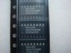
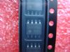
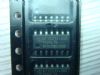
The LM293DR2 is a Low Offset Voltage Dual Comparator. The LM293DR2 is capable of single or split supply operation. It is designed to permit a common mode range-to-ground level with single supply operation. Input offset voltage specifications as low as 2.0 mV make the LM293DR2 an excellent selection for many applications in consumer, automotive, and industrial electronics.
Parametrics
LM293DR2 absolute maximum ratings: (1)Power Supply Voltage VCC: +36 or ±18 Vdc; (2)Input Differential Voltage Range VIDR: 36 Vdc; (3)Input Common Mode Voltage Range VICR -0.3 to +36 Vdc; (4)Output Short Circuit-to-Ground: Continuous mA; (5)Output Sink Current (Note 1): 20mA; (6)Power Dissipation @ TA = 25℃: 570mW; (7)Derate above 25℃: 5.7mW/℃; (8)Operating Ambient Temperature Range: -25℃ to +85℃; (9)Maximum Operating Junction Temperature: 150℃; (10)Storage Temperature Range Tstg: -65℃ to +150℃; (11)ESD Protection at any Pin Human Body Model: 2000V.
Features
LM293DR2 features: (1)Wide Single-Supply Range: 2.0 Vdc to 36 Vdc; (2)Split-Supply Range: ±1.0 Vdc to ±18 Vdc; (3)Very Low Current Drain Independent of Supply Voltage: 0.4 mA; (4)Low Input Bias Current: 25nA; (5)Low Input Offset Current: 5.0nA; (6)Low Input Offset Voltage: 5.0mV (max) LM293/393; (7)Input Common Mode Range to Ground Level; (8)Differential Input Voltage Range Equal to Power Supply Voltage; (9)Output Voltage Compatible with DTL, ECL, TTL, MOS, and CMOS Logic Levels; (10)ESD Clamps on the Inputs Increase the Ruggedness of the Device; (11)without Affecting Performance; (12)NCV Prefix for Automotive and Other Applications Requiring Site and Control Changes; (13)Pb-Free Packages are Available.
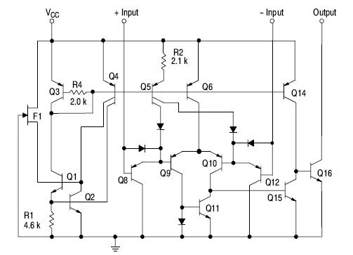
Diagrams
| Image | Part No | Mfg | Description |  |
Pricing (USD) |
Quantity | ||||||||||||
|---|---|---|---|---|---|---|---|---|---|---|---|---|---|---|---|---|---|---|
 |
 LM293DR2 |
ON Semiconductor |
Comparator ICs 2-36V Dual |
Data Sheet |
Negotiable |
|
||||||||||||
|
LM293DR2G |
ON Semiconductor |
Comparator ICs 2-36V Dual -25 to 85 deg C |
Data Sheet |
|
|
||||||||||||