(China (Mainland))


Product Summary
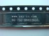
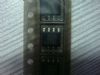
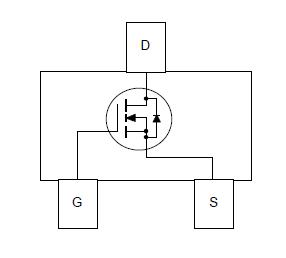
The NDS355AN is a N-Channel logic level enhancement mode power field effect transistor. It is produced using Fairchild’s proprietary, high cell density, DMOS technology. This very high density process is especially tailored to minimize on-state resistance. The NDS355AN is particularly suited for low voltage applications in notebook computers, portable phones, PCMCIA cards, and other battery powered circuits where fast switching, and low in-line power loss are needed in a very small outline surface mount package.
Parametrics
NDS355AN absolute maximum ratings: (1)Drain-Source Voltage: 30 V; (2)VGSS Gate-Source Voltage - Continuous: ±20 V; (3)ID Maximum Drain Current - Continuous: 1.7 A, Pulsed: 10 A; (4)PD Maximum Power Dissipation: 0.5 W; (5)Operating and Storage Temperature Range: -55 to 150 ℃; (6)Thermal Resistance, Junction-to-Ambient: 250 ℃/W; (7)Thermal Resistance, Junction-to-Case: 75 ℃/W.
Features
NDS355AN features: (1)1.7A, 30 V, RDS(ON) = 0.125 W @ VGS = 4.5 V, RDS(ON) = 0.085 W @ VGS = 10 V; (2)Industry standard outline SOT-23 surface mount package using proprietary SuperSOT-3 design for superior thermal and electrical capabilities; (3)High density cell design for extremely low RDS(ON); (4)Exceptional on-resistance and maximum DC current capability; (5)Compact industry standard SOT-23 surface mount package.
Diagrams
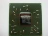
| Image | Part No | Mfg | Description |  |
Pricing (USD) |
Quantity | ||||||||||||
|---|---|---|---|---|---|---|---|---|---|---|---|---|---|---|---|---|---|---|
 |
 NDS355AN |
Fairchild Semiconductor |
MOSFET SOT-23 N-CH LOGIC |
Data Sheet |
|
|
||||||||||||
 |
NDS355AN_Q |
Fairchild Semiconductor |
MOSFET N-Channel Logic |
Data Sheet |
|
|
||||||||||||